Home > SUNTABA vacuum pallets applications > Thin PCB / FPC process
thin pcb/fpc applications
「SUNTABA vacuum pallets」complies with SGS's RoHS 2.0, PFOS, PFOA, and halogen-free environmental testing standards.
Just set it! The best solution for thin PCB and FPC production!
Due to the thin profile of mobile devices, circuit boards (PCB, substrate, FPC) are getting thinner and thinner.
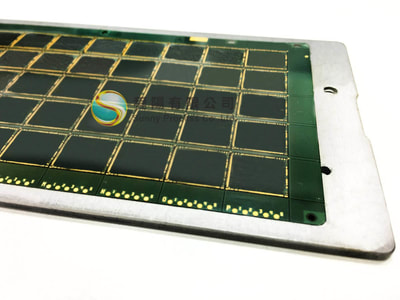
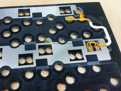
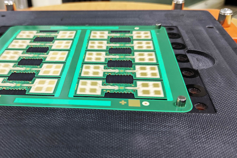
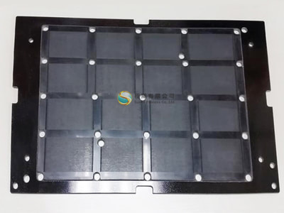
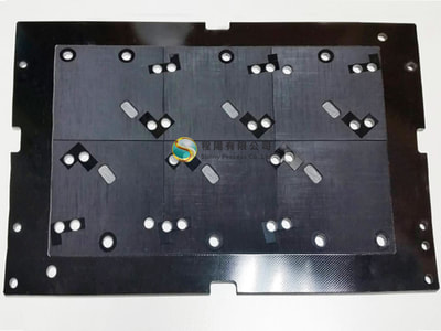
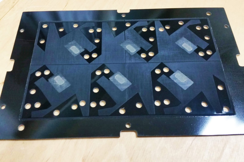
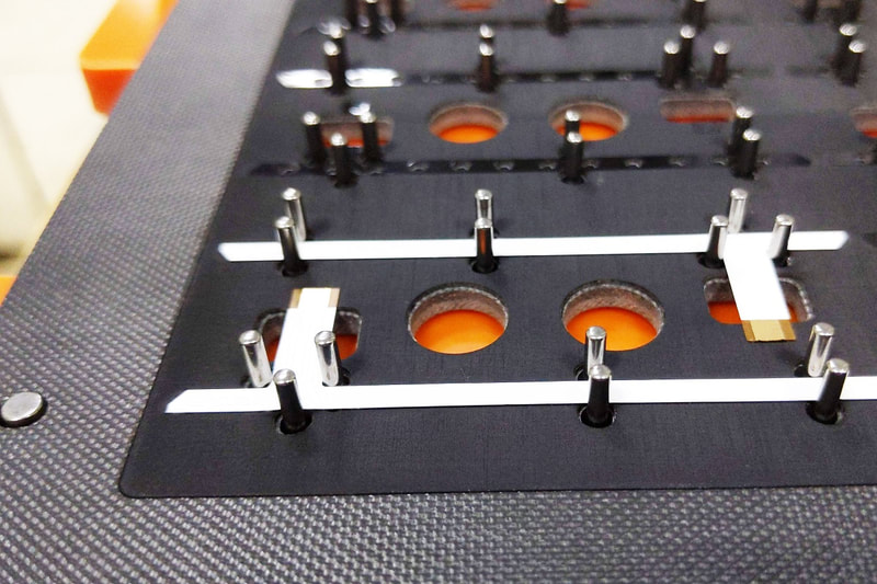
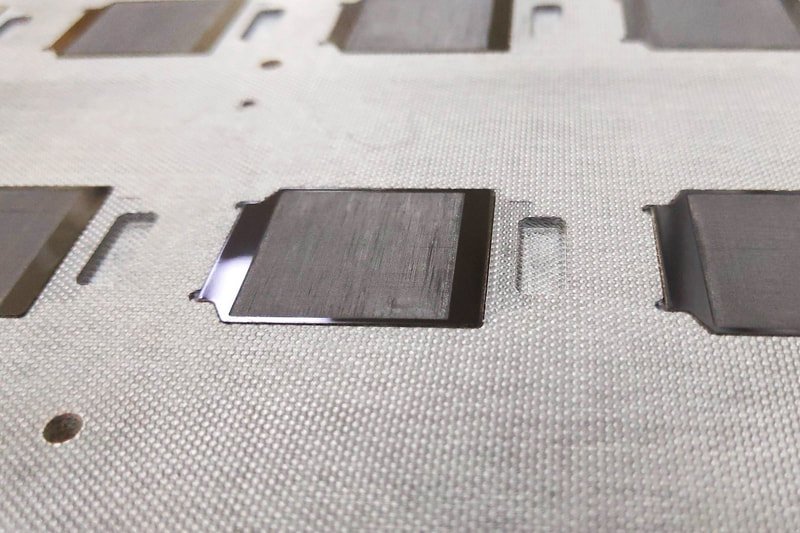
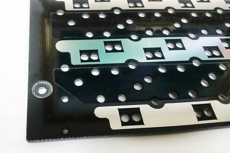
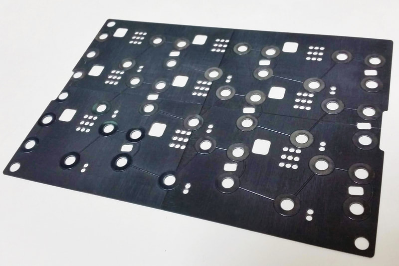
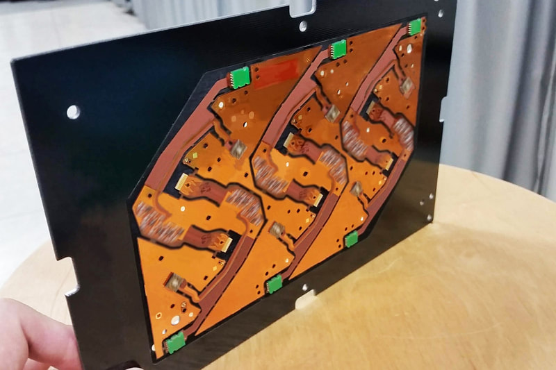
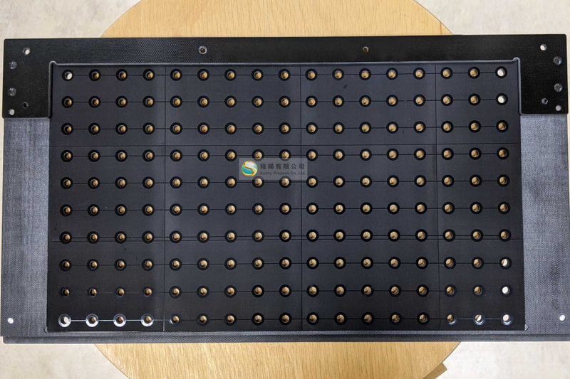
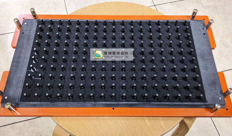
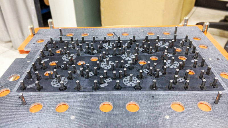
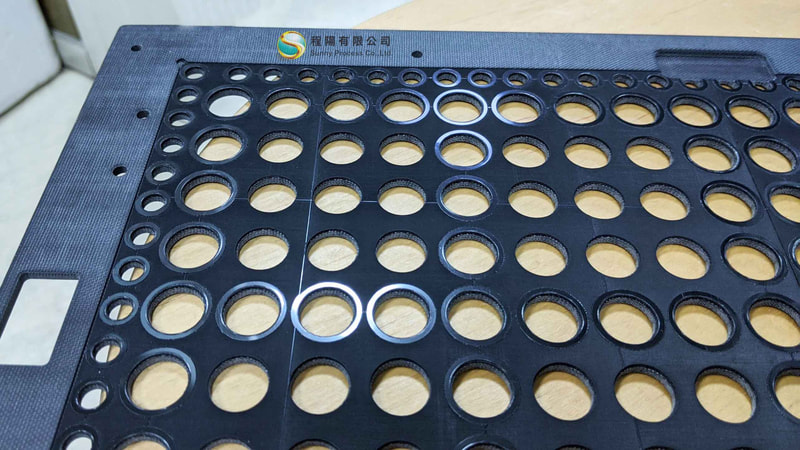
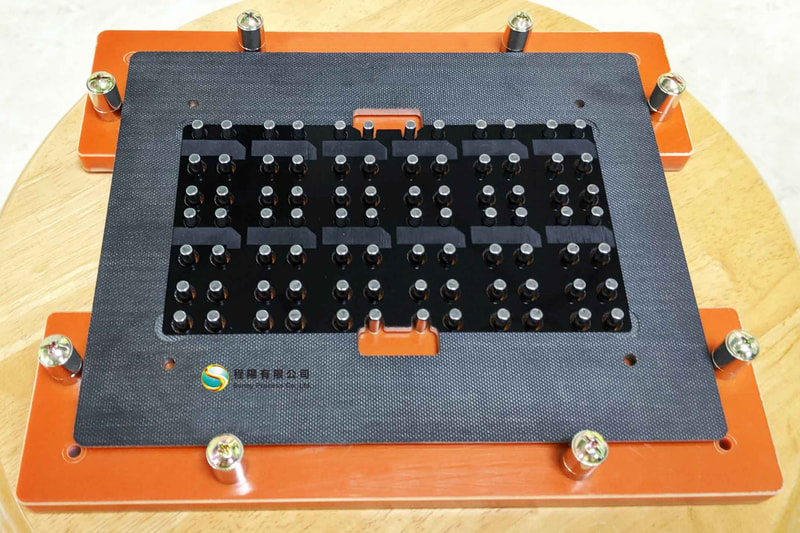
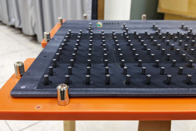
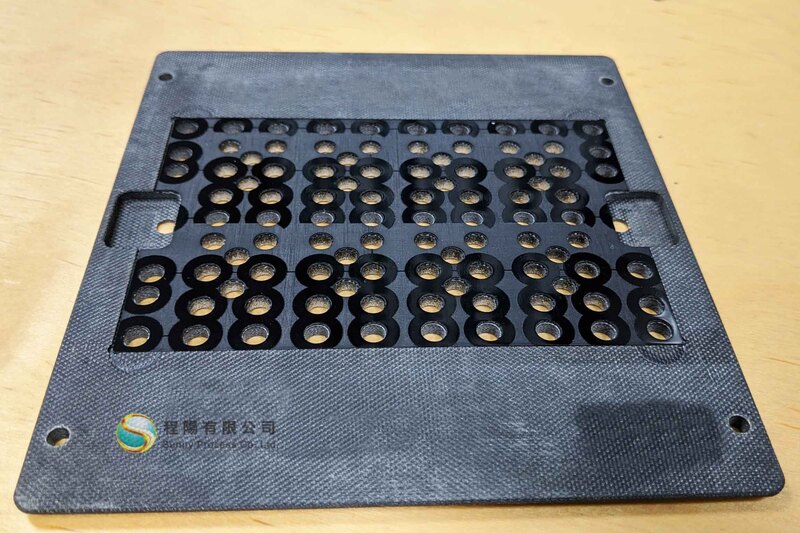
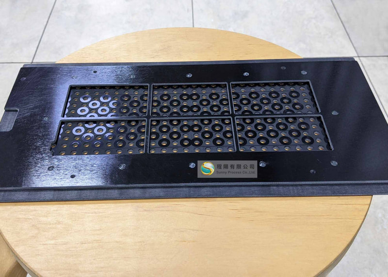
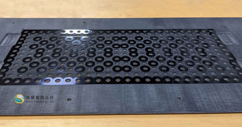
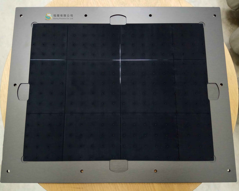
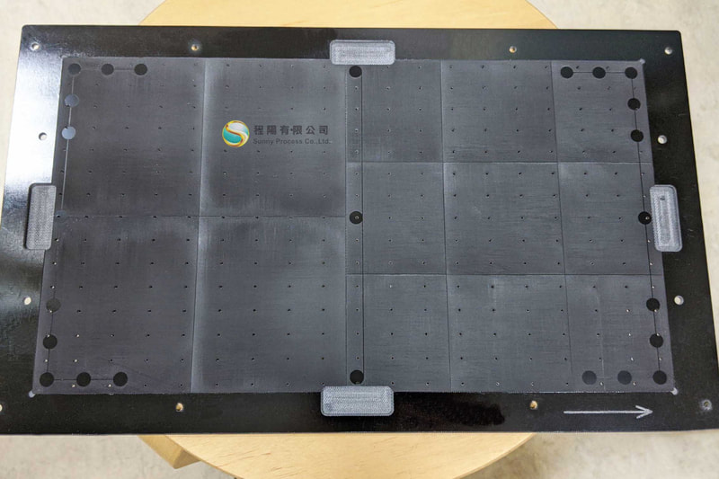
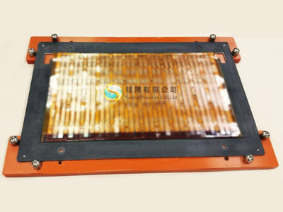
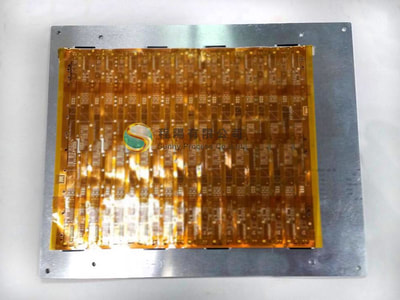
Thin PCB generally refers to the SMT process, with less than 0.6mm thickness. Commonly used materials include FR4, FPC, PI, PET, such as RFID, SD CARD, FLASH, FPC, COF ... etc. As shown in the picture, Suntaba Vacuum pallets can resolve the production problems of these substrates.
Due to the thin profile of mobile devices, circuit boards (PCB, substrate, FPC) are getting thinner and thinner.
- So how can we prevent deformation when producing ultra-thin PCB?
- How do we fix the board into position and remove the PCB when it is so thin?
- How do we automate the production of thin PCB?
Thin PCB generally refers to the SMT process, with less than 0.6mm thickness. Commonly used materials include FR4, FPC, PI, PET, such as RFID, SD CARD, FLASH, FPC, COF ... etc. As shown in the picture, Suntaba Vacuum pallets can resolve the production problems of these substrates.
- Reduces deformation of the PCB and improves the yield of the assembly.
- Reusable, reduces emissions and is environmentally friendly.
- Enhances automation and reduces manpower needs.
- Panelized production for enhanced efficiency.

